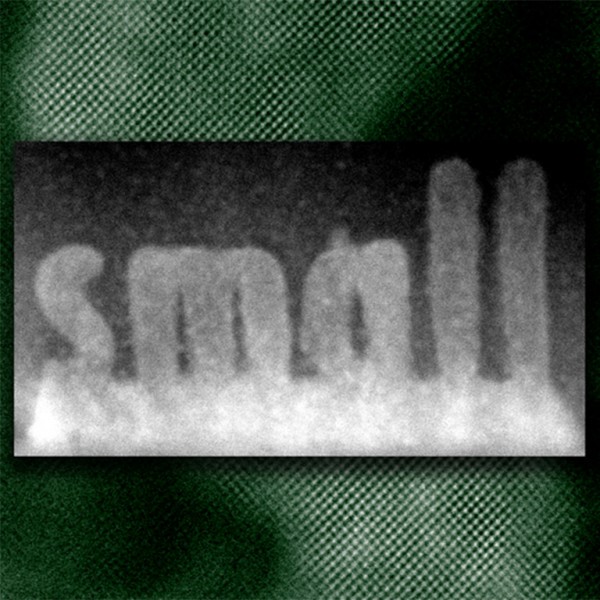
A team led by scientists at the Oak Ridge National Laboratory are combining the focused electron beam in a scanning transmission electron microscope with new electronic controls, allowing the atomic sculpting of crystalline material from non-crystalline material and the construction of 3D feature sizes down to one to two nanometers, less that the width of a strand of DNA, according to a statement by the Department of Energy, Office of Science.
The crystalline features have a particular alignment with the underlying atoms, allowing mechanical and electrical properties to extend throughout the material.
The electron beam in a scanning transmission electron microscope has been controlled with specially programmed electronics to tunnel into non-crystalline material and construct 3D features that are in perfect alignment with the underlying substrate (i.e., epitaxial). The result is designer materials with desirable structures, such as microchips, or materials with unique properties. Essentially, any shape can be created by exposing patterned areas to higher numbers of electrons than non-patterned areas, resulting in epitaxial 3D features down to one to two nanometers, according to the statement.
The crystalline features have a particular alignment with the underlying atoms, allowing mechanical and electrical properties to extend throughout the material. The electron beam from the scanning transmission electron microscope sculpted with atomic precision a crystalline oxide feature from a non-crystalline oxide layer on a crystalline substrate.
Nanofabrication with atomic-level sculpting can lead to new 3D materials for integrated circuits as well as new fundamental experimental studies ranging from crystallization to diffusion that can complement modeling and simulation.
The work was supported by the U.S. Department of Energy (DOE), Office of Science, Office of Basic Energy Sciences; the Center for Nanophase Materials Sciences and the Oak Ridge Leadership Computing Facility, DOE Office of Science User Facilities; and Laboratory Directed Research and Development Program at Oak Ridge National Laboratory.
[Image courtesy: Oak Ridge National Laboratory]

